Electrical and Photonic Interconnect Technologies
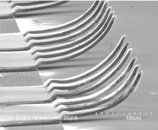
Heterogeneous integration of electronics and photonics is a promising solution to meet the high-bandwidth, low-latency, and low-energy consumption needs of modern computing systems, both for within- and off-package communication. Compared to electrical links, optical interconnects, which have many practical benefits such as high bandwidth density, low energy dissipation, and low communication latency, offer a promising solution for large-scale electronic integration. Within package photonic connectivity will be met with planar photonic links co-integrated with ultra-dense electrical interconnect network. Further, optical fibers, which offer extremely low loss, are especially critical in long-haul applications as well as in the shorter distances found in data centers and in high-performance computing (HPC). Photonic packaging, assembly, and interfacing with silicon electronics play a critical role in determining overall module performance, energy consumption, and cost. In order to create seamless polylithic integration of photonics and electronics, advances in packaging and assembly are critical. In particular, the accurate alignment and assembly of fibers or fiber arrays to a photonic integrated circuit (PIC) are crucial steps to realize high-efficiency optical packaging and integration. Moreover, the use of dense compressible microinterconnects as rematable interface between chiplets provides a number of practical benefits. The research in this thrust focuses on new photonic and electrical interconnects, fiber array alignment using microfabricated technologies, self-aligning chiplet assembly, and co-packaging of photonics and electronics.